Purpose
The RT6248B is an advanced constant on-time (ACOT™) mode synchronous buck converter with the input voltage range from 4.5V to 18V and provides 8A output current. This document explains the function and use of the RT6248B evaluation board (EVB), and provides information to enable operation, modification of the evaluation board and circuit to suit individual requirements.
Introduction
General Product Information
The RT6248B is an advanced constant on-time (ACOT™) mode synchronous buck converter. The main control loop of the RT6248B using an advanced constant on-time (ACOT™) mode control which provides a very fast transient response. The RT6248B operates from 4.5V to 18V input voltage, the output voltage can be programmed between 0.6V to 5.1V.
Product Feature
- Input Voltage Range : 4.5V to 18V
- 8A Output Current
- ACOT™ Mode Performs Fast Transient Response
- ACOT™ Architecture to Enable All MLCC Output Capacitor Usage
- Fixed 500kHz Switching Frequency
- High Efficient Internal Power MOSFET Switch 24mΩ (High-Side) and 12mΩ (Low-Side)
- Adjustable Output Voltage from 0.6V to 5.1V
- Pre-biased Soft-Start
- Cycle-by-Cycle Over-Current Protection
- Input Under-Voltage Lockout
- Thermal Shutdown Protection
- Output Over/Under-Voltage Protection
Key Performance Summary Table
|
Key Features
|
Evaluation Board Number: PCB091_V1
|
|
Default Input Voltage
|
12V
|
|
Max Output Current
|
8A
|
|
Default Output Voltage
|
3.3V
|
|
Default Marking & Package Type
|
RT6248BHGQUF, UQFN-12HL 3x3 (FC)
|
|
Operation Frequency
|
Steady 500kHz at all loads
|
Bench Test Setup Conditions
Headers Description and Placement
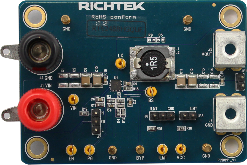
Carefully inspect all the components used in the EVB according to the following Bill of Materials table, and then make sure all the components are undamaged and correctly installed. If there is any missing or damaged component, which may occur during transportation, please contact our distributors or e-mail us at evb_service@richtek.com.
Test Points
The EVB is provided with the test points and pin names listed in the table below.
|
Test point/
Pin name
|
Signal
|
Comment (expected waveforms or voltage levels on test points)
|
|
VIN
|
Input voltage
|
Power input. Support 4.5V to 18V Input Voltage. Must bypass with a suitable large ceramic capacitor at this pin.
|
|
EN
|
Enable test point
|
Enable control. Pull this pin high to turn on the Buck. Do not leave this pin floating.
|
|
GND
|
Ground
|
Ground.
|
|
PGOOD
|
Power good test point
|
Power good Indicator. Open drain output when the output voltage is within 90% to 120% of regulation point.
|
|
FB
|
Feedback voltage input
|
The pin is used to set the output voltage of the converter to regulate to the desired voltage via a resistive divider. Feedback reference = 0.6V.
|
|
VCC
|
Internal regulator output
|
5V linear regulator Output for Internal Control Circuit. A capacitor (typical 1µF) should be connected to AGND. Don’t connect to external Load.
|
|
BOOT
|
Bootstrap supply test point
|
Bootstrap supply for high-side gate driver. Connect a 0.1µF ceramic apacitor between the BOOT and SW pins.
|
|
LX
|
Switch node test point
|
Connect this pin to an external L-C filter.
|
|
BYP
|
Bypass test point
|
Bypass input for the internal LDO. BYP is externally connected to the output of switching regulator. When the BYP voltage rises above the bypass switch turn-on threshold, the LDO regulator shuts down and the VCC pin is connected to the BYP pin through an internal switch.
|
|
ILIMT
|
Current limit seeting
|
Current limit setting pin. The current limit is set to 8A, 10A or 12A when this pin is pull low, floating or pull high respectively.
|
Power-up & Measurement Procedure
1. Connect input power (4.5V < VIN < 18V) and input ground to VIN and GND test pins respectively.
2. Connect positive end and negative terminals of load to VOUT and GND test pins respectively.
3. Set the jumper at J7 to connect terminals 2 and 3, connecting EN to VIN through resistor REN, to enable operation.
4. Verify the output voltage (approximately 3.3V) between VOUT and GND.
5. Connect an external load up to 8A to the VOUT and GND terminals and verify the output voltage and current.
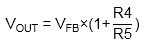
Output Voltage Setting
Set the output voltage with the resistive divider (R4, R5) between VOUT and GND with the midpoint connected to FB. The output is set by the following formula:
Schematic, Bill of Materials & Board Layout
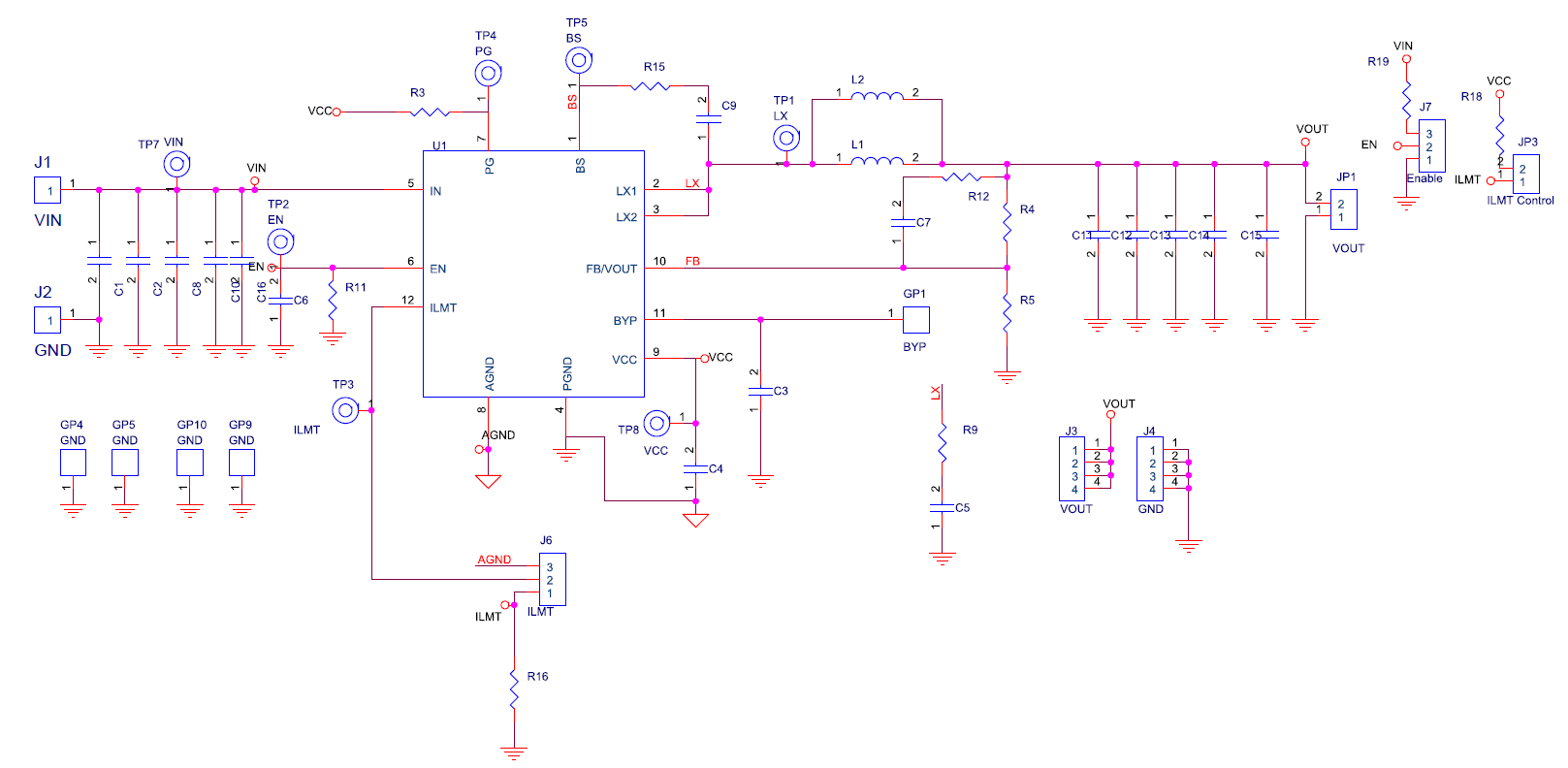
EVB Schematic Diagram
Bill of Materials
|
Reference
|
Qty
|
Part Number
|
Description
|
Package
|
Manufacturer
|
|
U1
|
1
|
RT6248BHGQUF
|
DC-DC Converter
|
UQFN-12HL 3x3 (FC)
|
RICHTEK
|
|
C3
|
1
|
C1608X5R0J475KT
|
4.7µF/6.3V/0603
|
C-0603
|
TDK
|
|
C4
|
1
|
C1608X5R1E105KT000E
|
1µF/25V/X5R/0603
|
C-0603
|
TDK
|
|
C6, C9, C15, C16
|
4
|
C1608X7R1H104KT000N
|
0.1µF/50V/X7R/0603
|
C-0603
|
TDK
|
|
C7
|
1
|
0603N680J500
|
68pF/50V/NPO/0603
|
C-0603
|
WALSIN
|
|
C8, C10
|
2
|
UMK325BJ106MM
|
10µF/50V/X5R/1210
|
C-1210
|
TAIYO YUDEN
|
|
C11, C12
|
2
|
C3225X5R1E226MT
|
22µF/25V/X5R/1210
|
C-1210
|
TDK
|
|
L1
|
1
|
7443552150
|
1.5µH
|
L-GSCDK104
|
WE
|
|
R3, R19
|
2
|
WR06X1003FTL
|
100k/0603
|
R-0603
|
WALSIN
|
|
R4
|
1
|
RTT039092FTP
|
90.9k/0603
|
R-0603
|
WALSIN
|
|
R5
|
1
|
WR06X2002FTL
|
20k/0603
|
R-0603
|
WALSIN
|
|
R11
|
1
|
WR06X3602FTL
|
36k/0603
|
R-0603
|
WALSIN
|
|
R12, R15
|
2
|
WR06X000PTL
|
0R/0603
|
R-0603
|
WALSIN
|
|
R16
|
1
|
WR06X7502FTL
|
75k/0603
|
R-0603
|
WALSIN
|
|
R18
|
1
|
WR06X1002FTL
|
10k/0603
|
R-0603
|
WALSIN
|
PCB Layout
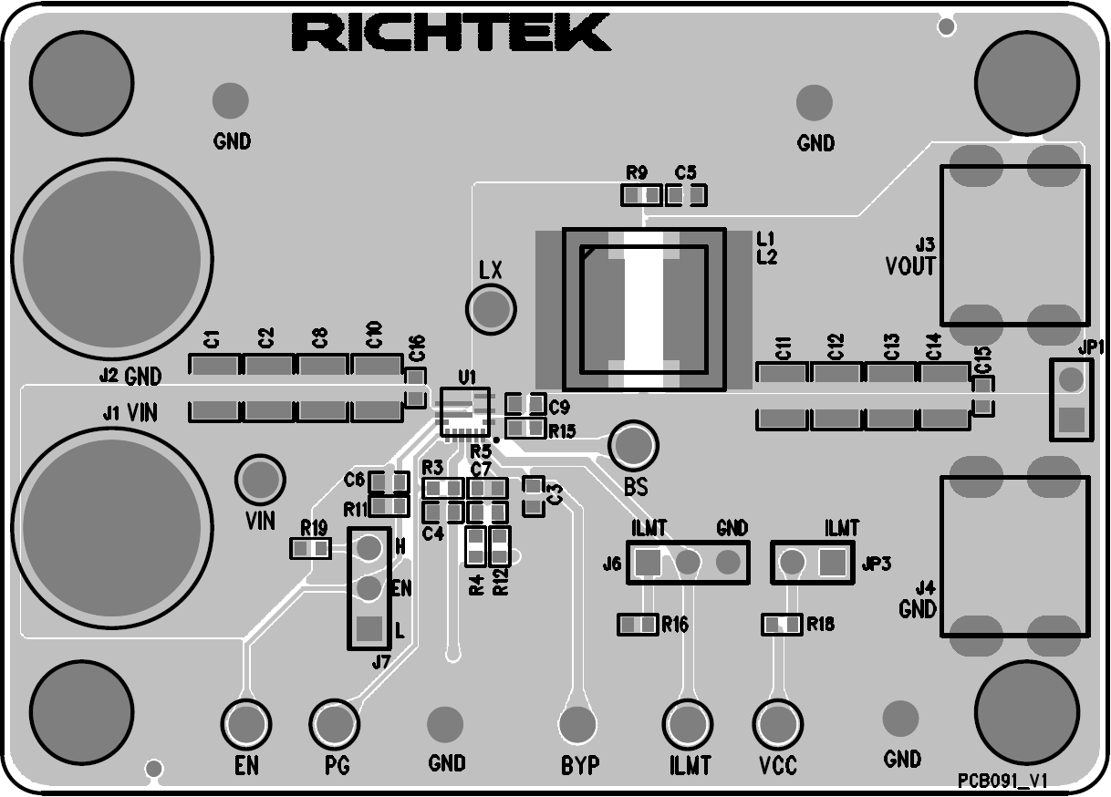
Top View (1st layer)

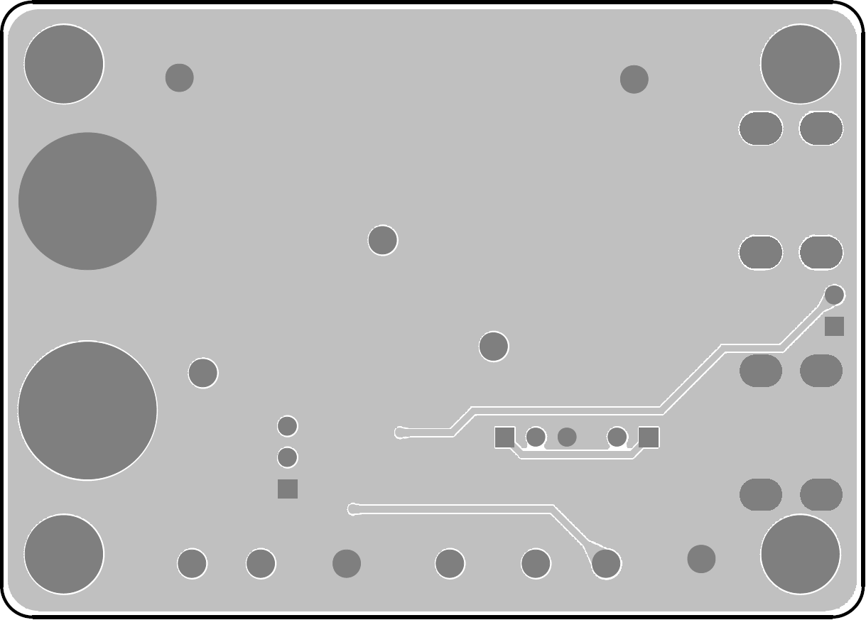
PCB Layout—Inner Side (2nd Layer)

PCB Layout—Inner Side (3rd Layer)
Bottom View (4th Layer)